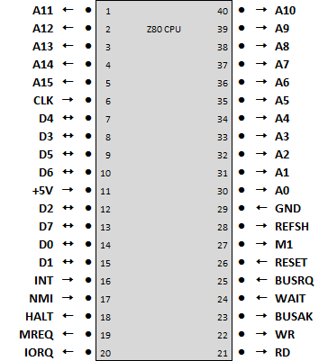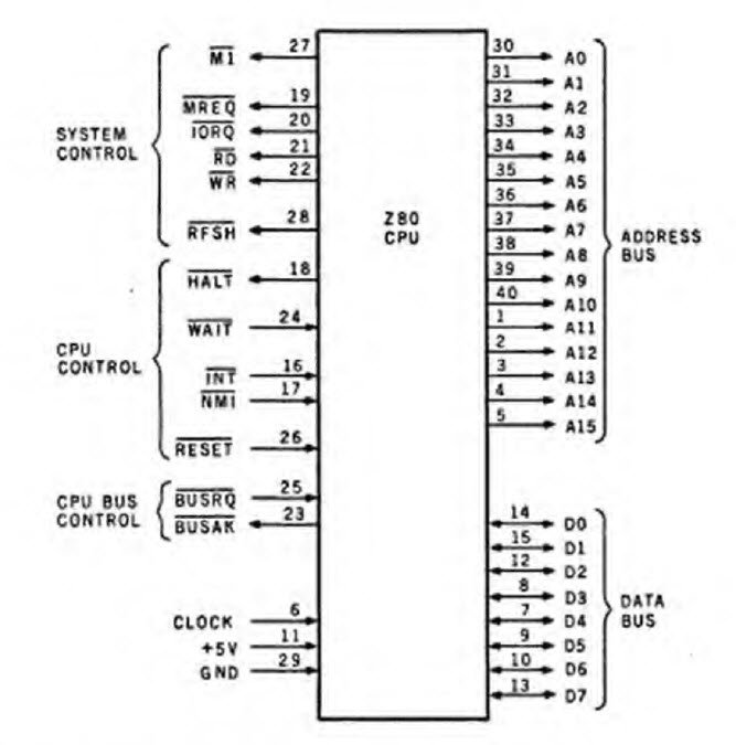

Z80 CPU Pinout Signal Functions
{Address Bus}
A0-A15 – Address bus output tri-state (active High) 16bit Address Bus, provides address for memory data exchanges (up to 64K) and for IO device data exchanges. For IO devices, only the eight lower addresses for 256 input or 256 output ports. During DRAM refresh times, the lower seven bits contain a valid refresh address.
{Data Bus}
DO-D7 – Data bus bidirectional tri-state (active High) – 8 bit data bus, bidirectional used for data exchanges with memory and IO devices.
{System Control}
M1- Output pulse on instruction fetch cycle(active Low)– Indicates that the current machine cycle is the operation-code fetch cycle of an instruction execute. M1 is generated when each opcode is fetched. M1 also is generated with IORQ to indicate an interrupt acknowledge cycle.
MREQ – {Memory Request} Memory operation status output tri-state (active Low) – Indicates that the address bus holds a valid address for a memory-read or memory-write operation.
IORQ – {Input/Output Request} IO operation status output tri-state (active Low)- indicates that the lower 8bits of the address bus holds a valid IO address for an IO read or write operation. An IORQ signal is generated with an M1 signal when an interrupt is being acknowledged to indicate that an interrupt response vector can be placed on the data bus.
RD – {Memory Read} outputs tri-state (active Low) – Indicates that the processor wants to read from Memory or IO Device. When RD signal is low – the addressed memory or IO Device should place the requested data on the data bus.
WR – {Memory Write) outputs tri-state (active Low) – Indicates that the data bus holds valid data to be stored in memory or IO device.
RFSH – {Refresh} – Dynamic memory refresh output (active Low) – Indicates that the lower seven bits of the address bus contain a refresh address for dynamic memories and the current MREQ signal should be used to do a refresh read to all dynamic memories.
{CPU Control}
HALT -{Halt State} – CPU halt status output (active Low) – Indicates that the CPU has executed a HALT instruction and is waiting for either a nonmaskable or maskable interrupt before operation can resume. When halted the CPU executes NOPs to maintain memory refresh activity.
WAIT – {Wait} – Wait request input (active Low) – Indicates to the CPU that the address memory or IO device is not ready for a data transfer. The CPU will stay in the wait state as long as WAIT is active. This signal allows memory or IO devices to be synchronized to the CPU.
INT – {Interrupt} – Interrupt request input (active Low) – The interrupt signal is generated by IO devices. A request will be processed at the end of the current instruction, if enabled by software and if the BUSRQ signal is not active. When the CPU accepts the interrupt and acknowledge signal IORQ during M1 time is sent out at the beginning of the next instruction cycle. The CPU can respond to the interrupt in three different modes.
NMI – Non-maskable interrupt input (active Low) – The non-maskable interrupt request line has a higher priority than INT and is always recognized at the end of the current instruction, regardless if interrupts are enabled or not. NMI forces the CPU to restart to location$0066. The program counter is automatically saved in the external stack. Continuous WAIT cycles can prevent the current instruction from ending and a BUSRQ will override an NMI.
RESET – Reset input (active Low) – initializes the CPU as follows: it resets the interrupt enable, clears the PC and registers I and R, and sets the interrupt status to Mode 0. During reset time, the address and data bus go to a high-impedance state, and all control output signals go to the inactive state. Notice that RESET must be active for a minimum of three full clock cycles before the reset operation is complete.
{CPU Bus Control}
BUSRQ – Bus request input (active Low) – Bus Request has a higher priority than NMI and is always recognized at the end of the current machine cycle. BUSREQ forces the CPU address bus, data bus, and control signals MREQ IORQ, RD, and WR to go to a high-impedance state so that other devices can control these lines. Extended BUSREQ periods due to extensive DMA operations can prevent the CPU from properly refreshing dynamic RAMS.
BUSAK – Bus acknowledge output (active Low) – Bus Acknowledge indicates to the requesting device that the CPU address bus, data bus, and control signals MREQ, IORQ RD, and WR have entered their high-impedance states. The external circuitry can now control these lines.
CLK – CPU Clock Input – Single-phase MOS-level clock.
Power supply inputs – +5 and GND.
Need a Creator Alchemist on Your Project?
I’m available for hire—consulting, systems design, embedded tech, creative problem-solving, or anything in between.
If you’ve got a project that needs someone who can think it through and build it out, I’m interested.
👉 Let’s Talk
jamie@jamiestarling.com
