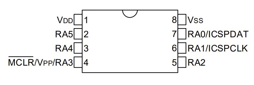
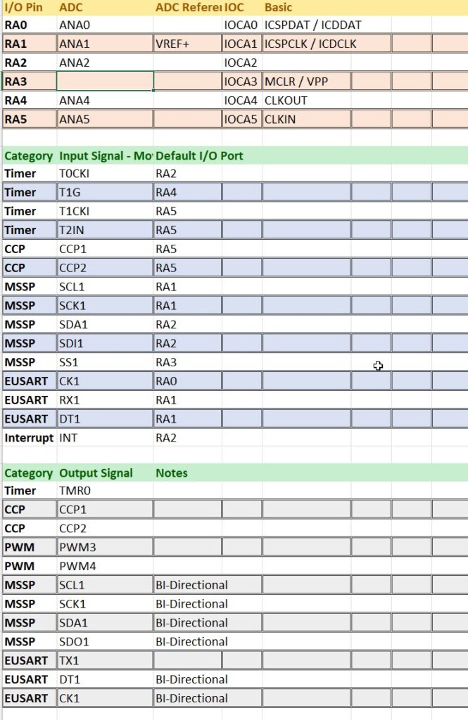
PIC16F15213 Pin Diagram – Image.

VSS – Ground
VDD – Operating Voltage Range: 1.8V to 5.5V
**NOTE RA3 – {MCLR} If used for IO is an input pin only! Cannot be used as Output. Cannot be used for Analog ADC
Pin descriptions and Pin Mappings

**Notes BI-Directional output signals need to be mapped to the same input signal
**Notes to use Output signals they have to be mapped to IO pin – as they do not have default assigned PIN.
Need a Creator Alchemist on Your Project?
I’m available for hire—consulting, systems design, embedded tech, creative problem-solving, or anything in between.
If you’ve got a project that needs someone who can think it through and build it out, I’m interested.
👉 Let’s Talk
jamie@jamiestarling.com
